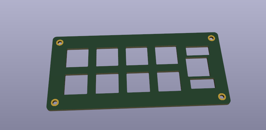
Keyboard Design Part 6 - On-Board MCU - Schematic Capture
Now that we've integrated somebody else's microcontroller board into a keyboard PCB, we should take a moment to learn about integrating microcontrollers directly into our keyboard PCBs.
Let's walk through the important steps of schematic capture before doing board layout!
The microcontroller I use for most of my PCBs is the RP2040 from the Raspberry Pi foundation. The highlights are:
- Dual-core Arm Cortex-M0+ processor, flexible clock running up to 133 MHz
- 264kB on-chip SRAM
- 2 × UART, 2 × SPI controllers, 2 × I2C controllers, 16 × PWM channels
- 1 × USB 1.1 controller and PHY, with host and device support
- 8 × Programmable I/O (PIO) state machines for custom peripheral support
- QMK/Via/Vial support
- External SPI flash required
This microcontroller has excellent community support and is relatively easy to integrate into a PCB. As compared to industry focused microcontrollers like ST's offerings (i.e. STM32F411's used in PCBs) the RP2040 requires a couple of extra components to function. As always, check the datasheet!
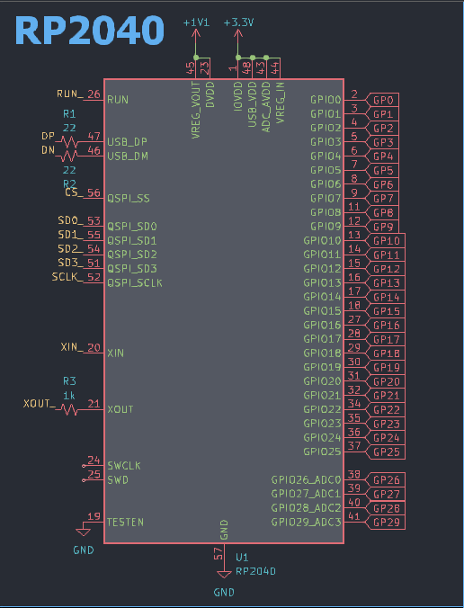
This is the heart of the keyboard! I use "Shift+L" to create node labels that make the schematic easier to read. Some critical things to note are:
- The RP2040 has an integrated 3.3V->1.1V regulator for internal use.
- The TESTEN pin must be shorted to ground.
- The RUN_ node should be connected to a button to allow restarting the board.
The RP2040 has a built in USB bootloader (which is not typical for most microcontrollers) that enables easy programming. If you need to do mass programming, you might prefer to expose the "SWCLK," "SWD," and "3.3V" pins.
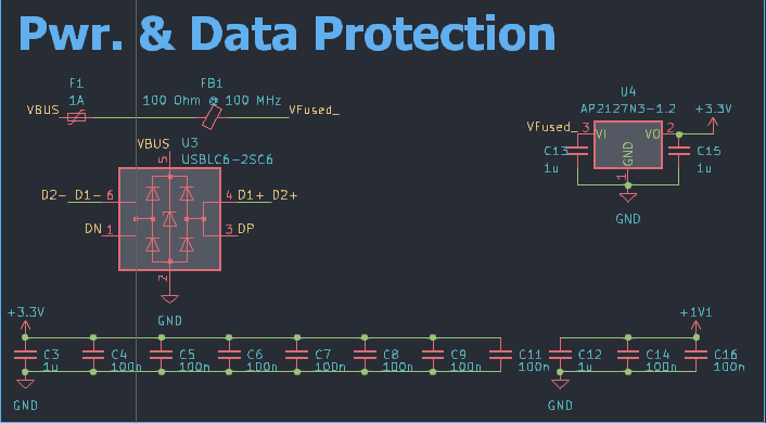
The RP2040 requires a number of decoupling capacitors for proper functioning. Check the last post on decoupling capacitors for more info! One 100nF cap is used per VDD input pin (as specified in the datasheet) and a bulk 1uF cap is used per voltage regulator.
Power is supplied to the microcontroller through USB. However, USB's nominal voltage (for our purposes!) is 5V. The AP2127N3-1.2 is an extremely common 3.3V fixed regulator that has, probably, a million clones available. This will take in our 5V and spit out 3.3V for the RP2040's regulators. Other things to note in this section are the USBLC6 ESD protection IC which protects the data and power lines of your USB port. A 1A PTC resettable fuse is included as well as a 100 Ohm @ 100 MHz ferrite bead. There is a lot of woo surrounding ferrite beads. I haven't done near field testing of any keyboard PCB but it is cheap to include a ferrite bead and can solve EMI issues. For more information check out StackExchange post:

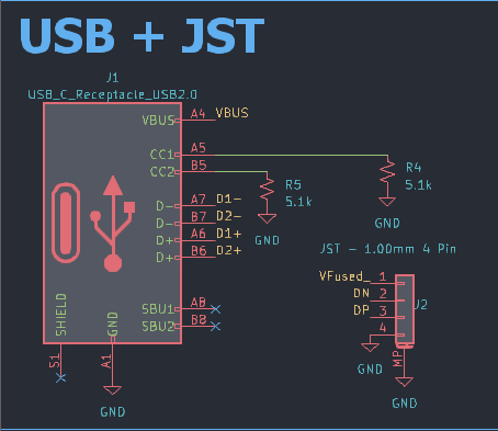
Next let's check out our PCB connectors. The USB-C port used has a few pins you may not be familiar with if you have previously used Micro-B USB ports. The CC1/CC2 pins are used for orientation detection. Only one pin is connected to the cable that is inserted. The 5.1k resistors "communicate" with the USB host that the peripheral is requesting a maximum of 500mA. The CC lines are used for USB power delivery. Thankfully, even the most severely gamerfied RGB keyboards should use less than 500mA. Your mileage may vary if you include a solenoid or 600 NeoPixels.
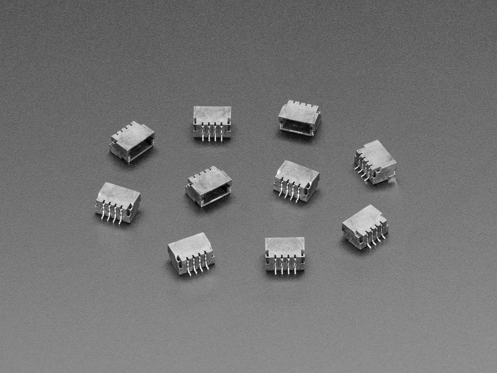
The other connector is a JST connector to be used with a Unified Daughter Board. This is for the JST variant (which shares cable specs with STEMMA Qt and Qwiic connectors).
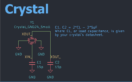
Next is the crystal. The RP2040, when it starts up, creates a clock signal using an internal oscillator (probably using an RC circuit). This is a clock signal that is too inaccurate for USB's strict timing tolerance! The RP2040 then starts driving its crystal which provides superior timing precision and allows USB to work well without a hitch. Quartz crystals require load capacitors. C1 = C2, C1 = 2*CL - 4pF should give you values in the ball park. CL is a value given by a crytal's datasheet.
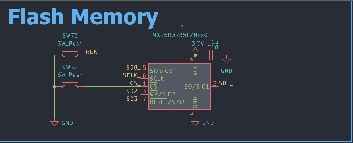
Next, here are the connections to the RP2040's external flash. A button is placed on the chip-select pin of the flash. When this button is held down, it forces the RP2040 to run it's ROM bootloader instead of the SPI flash's program code. This allows you to reprogram the device! The other button simply resets the RP2040.
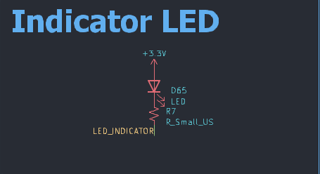
An indicator LED is provided as an example for a caps lock indicator. For more information on choosing an LED resistor value, check this post. The LED_INDICATOR net label should be applied to a GPIO pin of the microcontroller. In this configuration, the microcontroller will sink a significant amount of current (~5mA).
Do not exceed the rated current sink of the microcontroller! It will never be more than 20mA. If you need an array of LEDs consider using a dedicated LED driver or individual transistors.
Finally, there is the switch matrix.
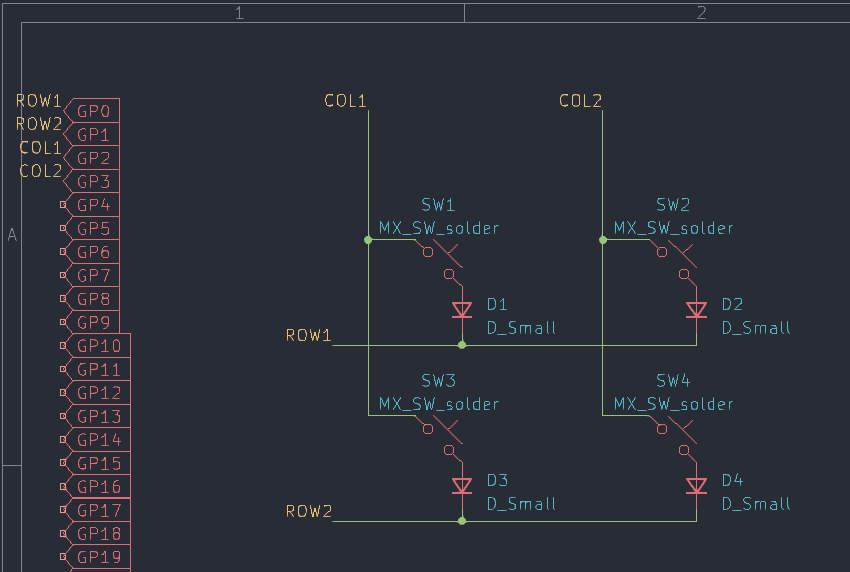
Each switch requires a diode. The microcontroller alternates what rows/columns are scanned--the diodes prevent "ghosting" and allow n-key rollover. This is just a small example, your matrix will likely have between 10-15 columns and 3-6 rows. Matrices are used in order to allow a microcontroller with relatively few pins (30 for the RP2040) to address many switches.
You can download this RP2040 template project here:
Thanks for reading!


