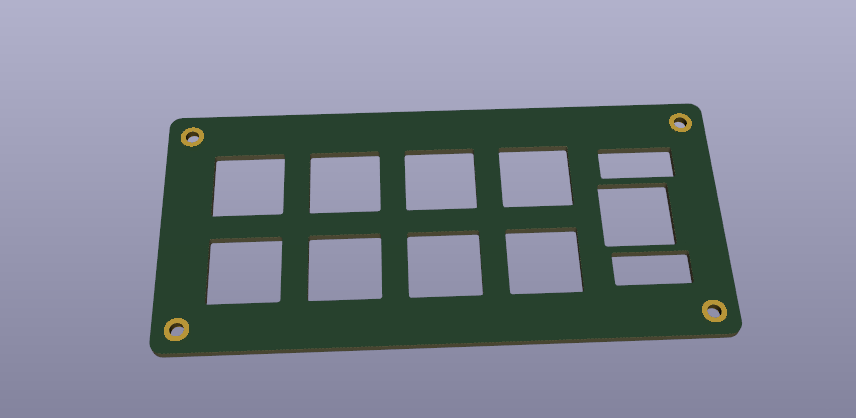
Keyboard Design Part 4 - PCB Layout
Time to design something you can really hold in your hand! If you've been following along, you should have a cool macropad layout planned and footprints for everything you need.
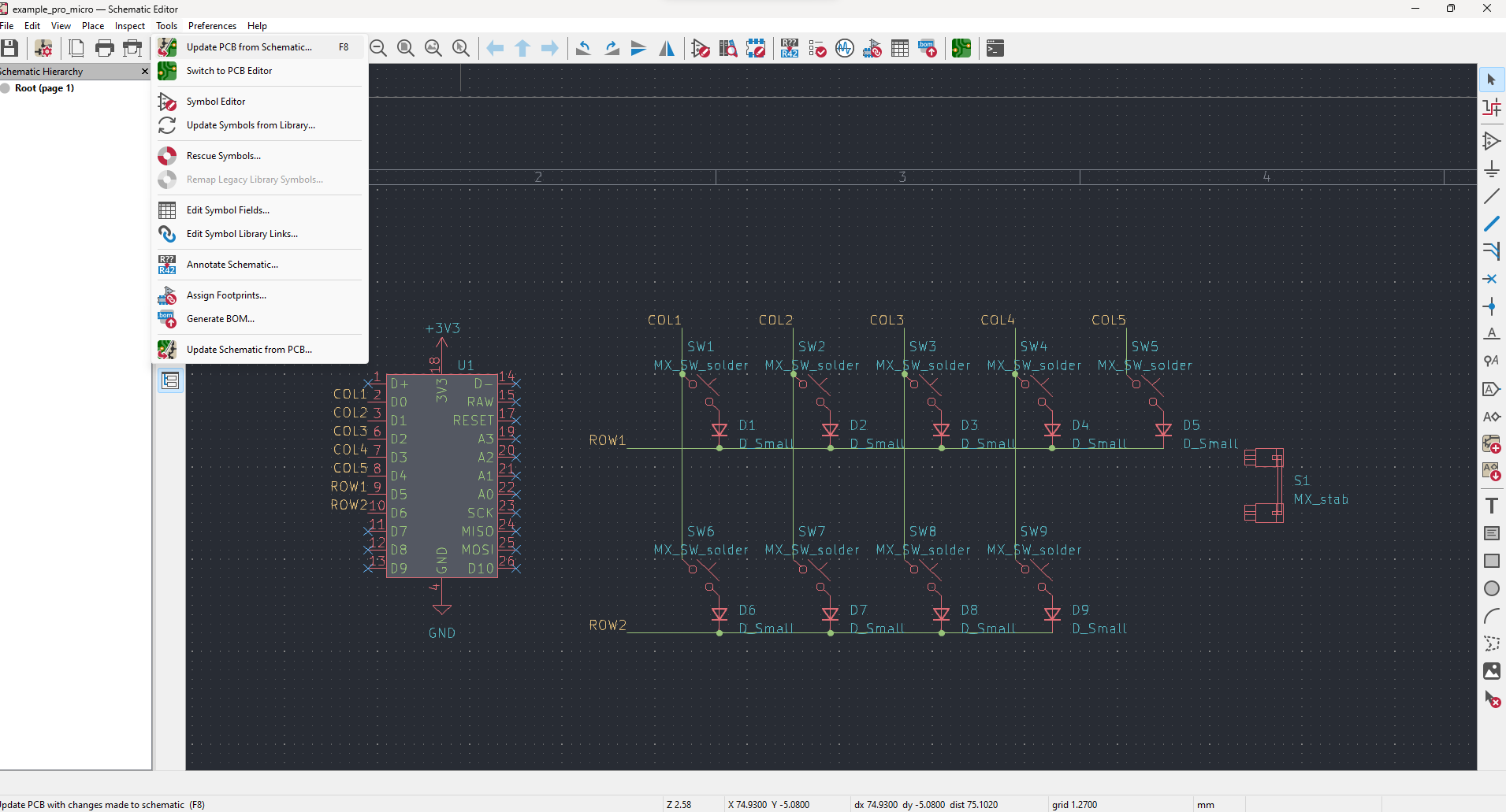
Click "Tools > Update PCB from Schematic." KiCAD should open up the PCB editor.
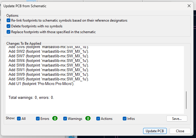
Keep everything checked for now. If you are updating a PCB from a schematic in the future you should look more carefully at these options.
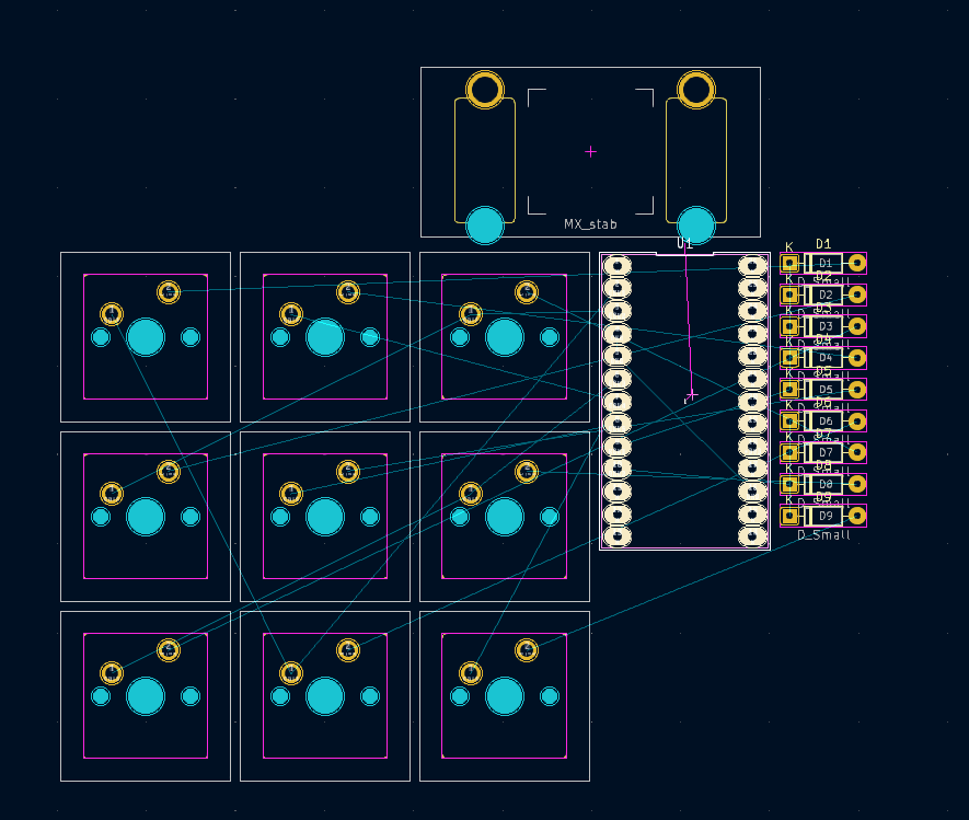
Nice! Keyboard switches are 0.75" or 19.05mm square. This is a bit of a simplification--keycaps are something close to 18mm square and plate cutouts are 14mm square.
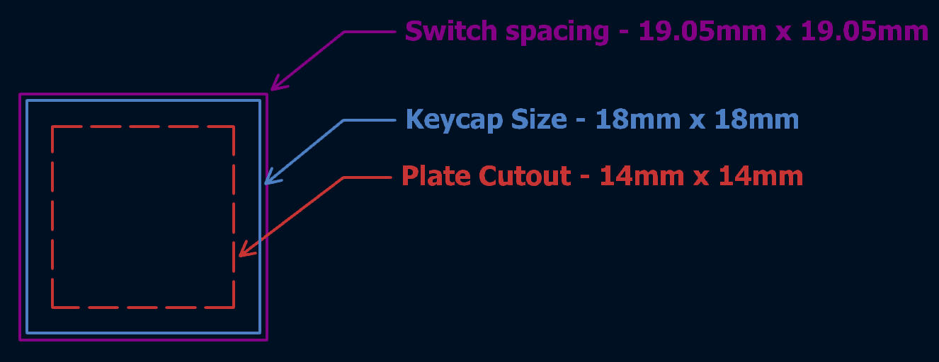
Here is a diagram of relevant keyswitch dimensions!
Let's set up the "snap grid" to fit keyboard switches.
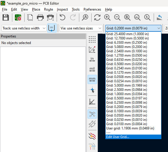
Click the grid drop-down. Click on "Edit User Grid..."
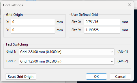
Enter 0.75" / x to get fractions of a key switch unit, commonly referred to as "u" (as in 2u, 6.25u, 10u keys). I personally use 16 as my divisor but you can use whatever you'd like!
Tip: KiCAD will evaluate unit conversions for you in most input boxes!
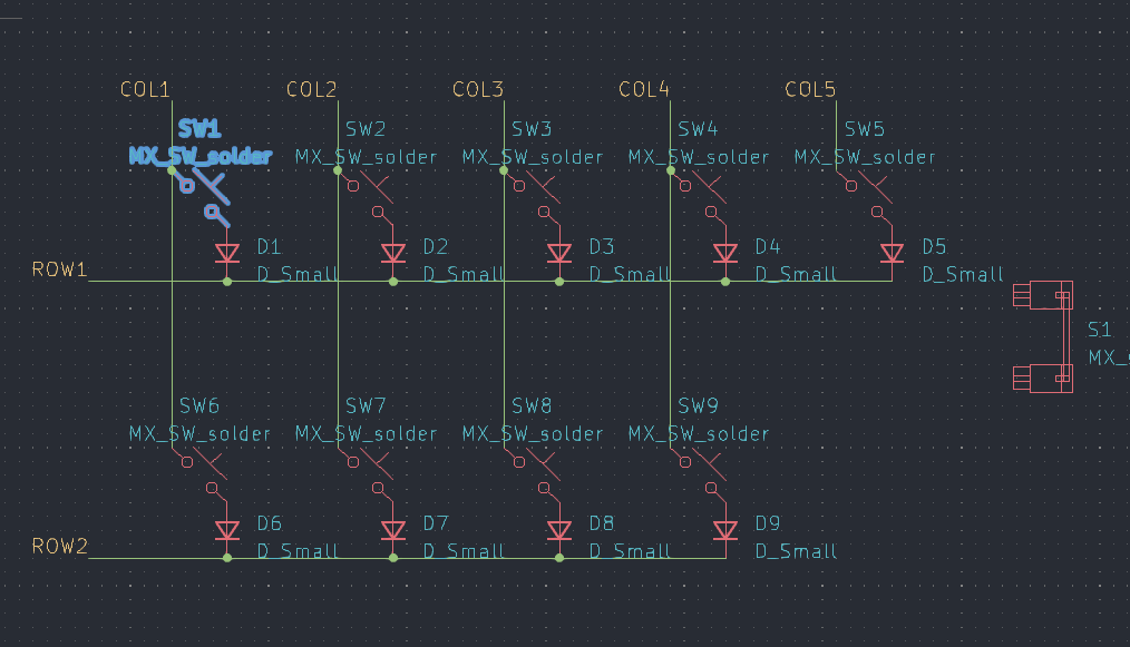
Click back and forth between the schematic and PCB to find footprints. This is what I do when not using an auto-placing script and I recommend you do it to get the hang of navigating between the schematic and PCB editor. When you click on a symbol in the schematic, it highlights its footprint in the PCB editor!
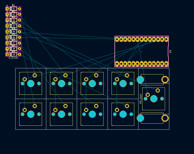
Once you have laid out your macropad's keys, you should see something like this.
Note: the stabilizer orientation changes the direction of the cutout you will use on the keyboard's plate.
Position your pro-micro somewhere nice looking. This will be relatively easy to route!
Place your diodes in a way that minimizes the number of crossing traces. This is an art! Don't worry if it isn't perfect, just make sure that everything connects properly.
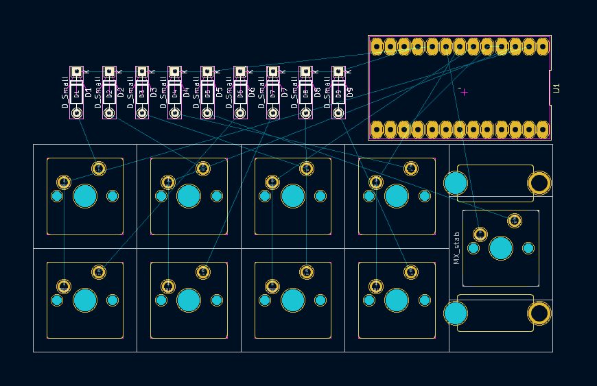
Next, press "X" to start routing. You're really doing it!
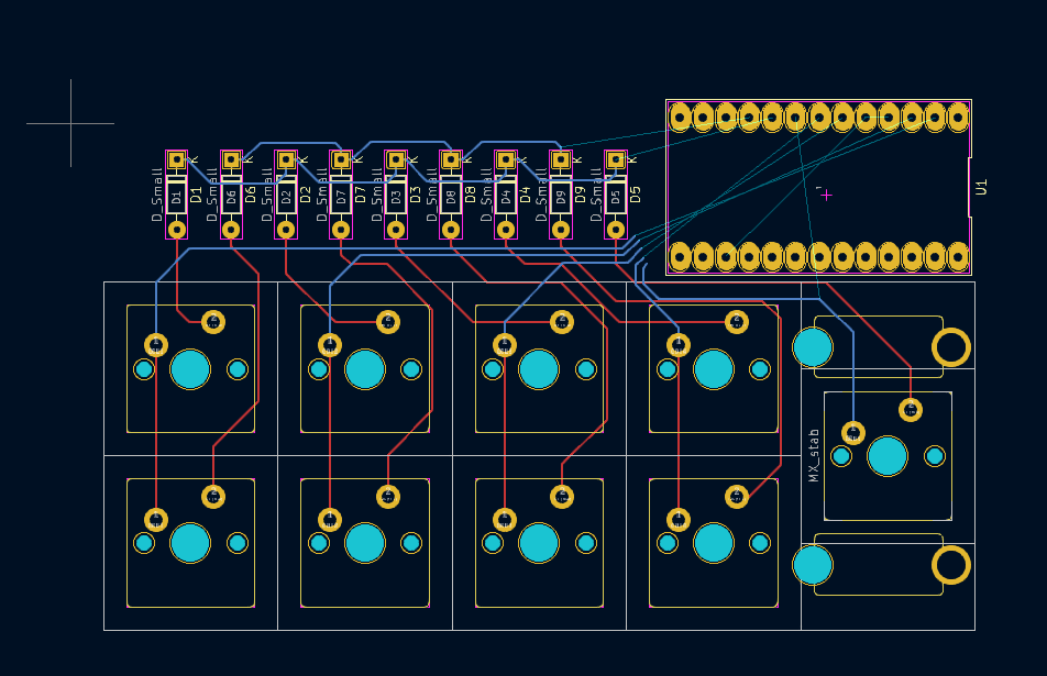
Here I am halfway through routing. Notice that the ratsnest (the little lines running between traces and their destinations) is crossing itself. Let's change some pin numbers around in the schematic to simplify this. Remember: we should only use pins labelled "D*" because these are available GPIOs on all pro micros.
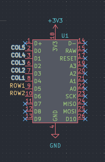
I've flipped the COL1-COL5 pins by selecting them and pressing "y" to flip vertically.
Be sure to update the PCB from the schematic in order to transfer these changes.
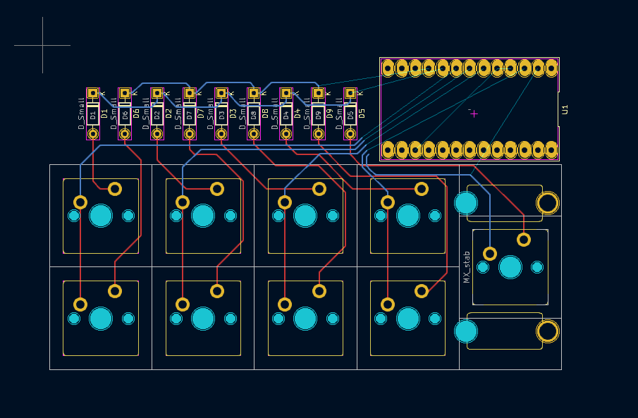
There! Much better.
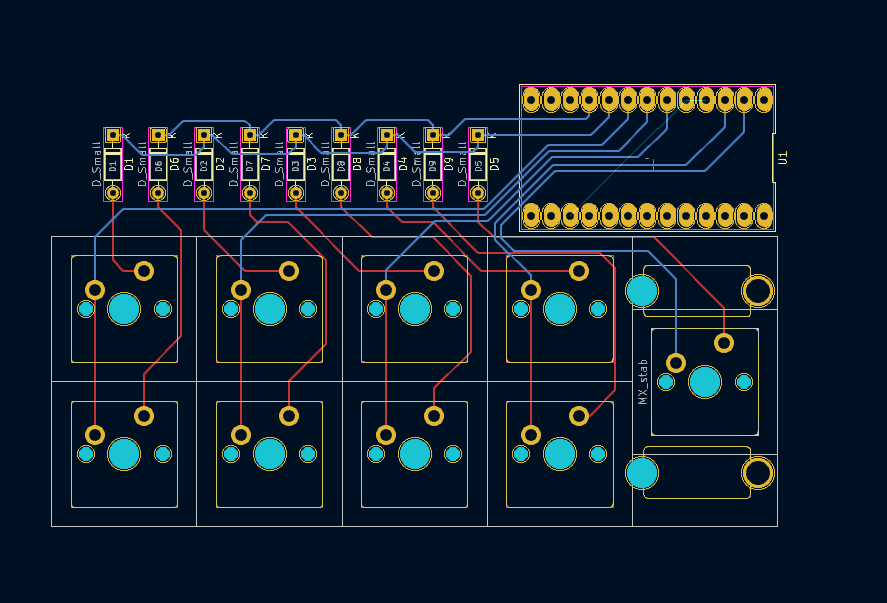
Routing complete! Let's take a look at its 3D render.
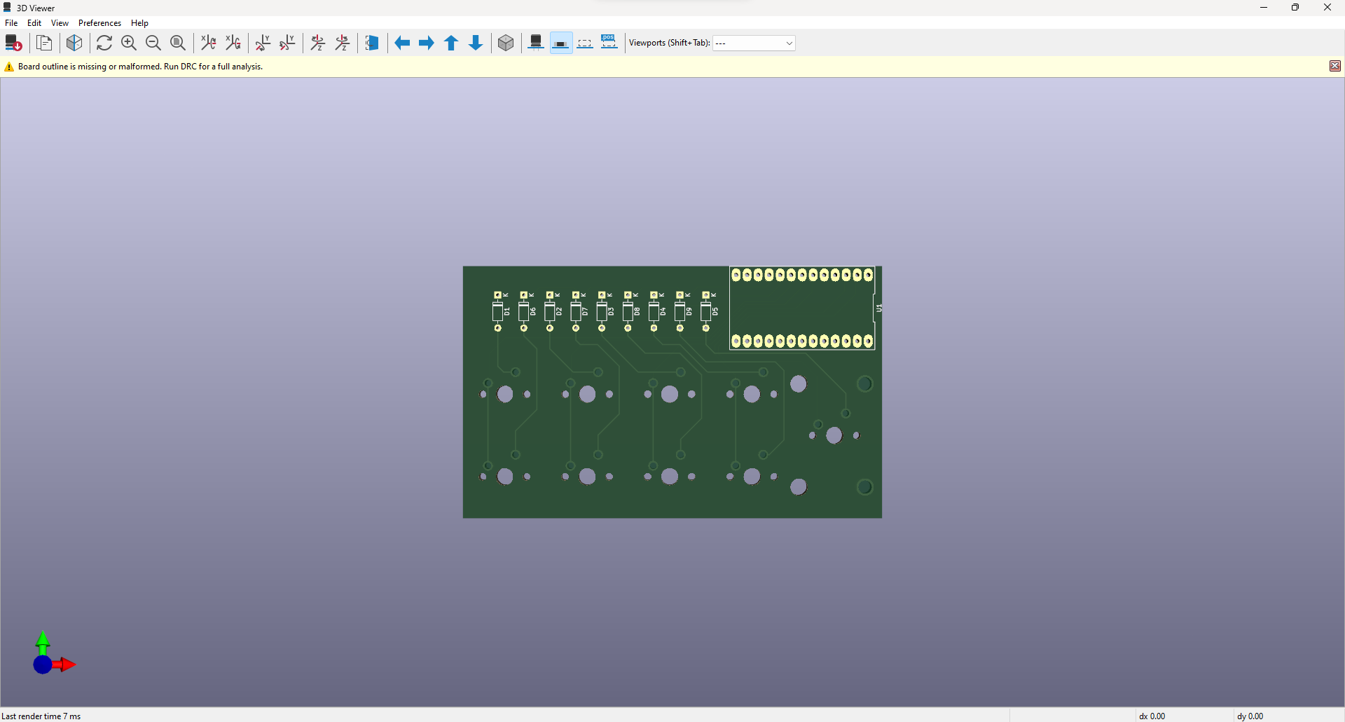
See that error? That means that we need to define the actual physical edges of our board by drawing them on the "edgecuts" layer. Let's define edgecuts for this board.

Select the "Edge.Cuts" layer. Switch your grid spacing to the key-unit size.
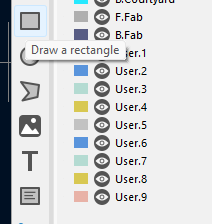
Next, select the rectangle tool in the toolbar to the right.
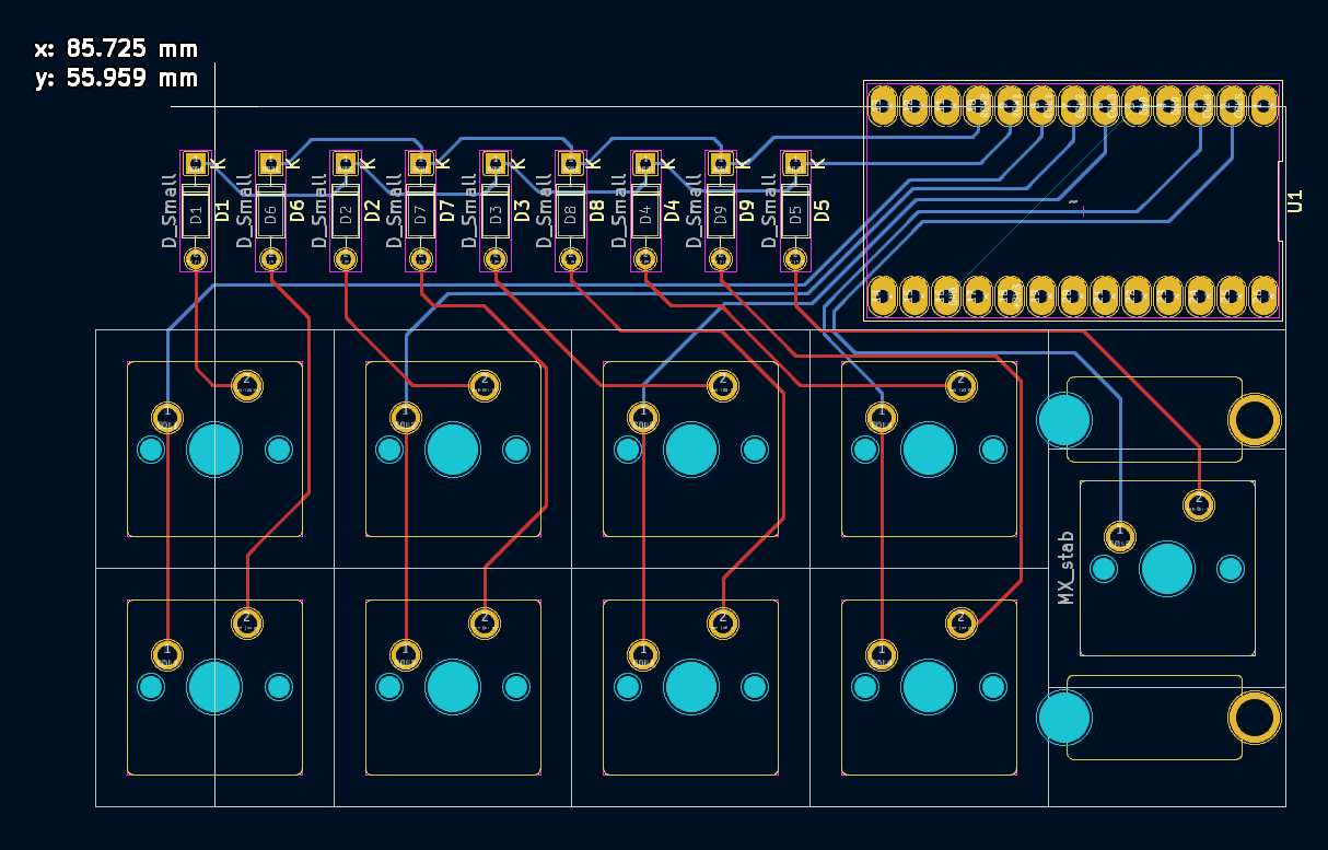
Draw out the edgecuts! I added a bit of extra distance up top.
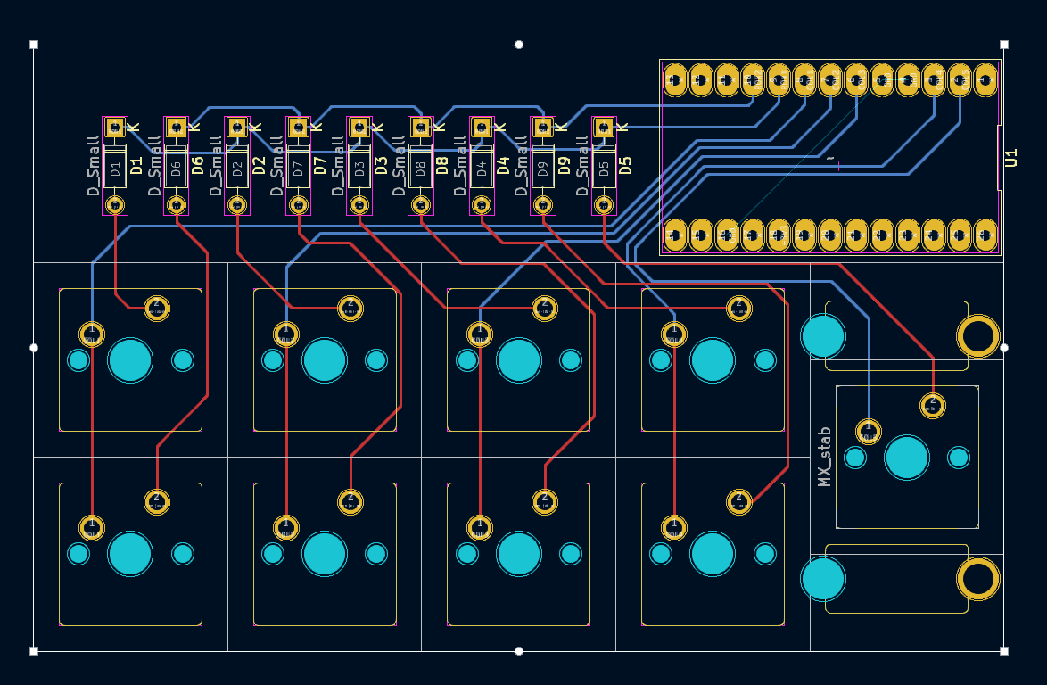
The edges are a bit sharp, though. If you were to order this board as-is, you would probably poke yourself on the edges. Let's add some fillets (aka radii) to the edges.
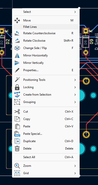
Right click the rectangle you created and "Fillet Lines."
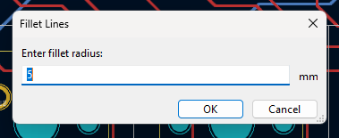
Set your radius to whatever you'd like. Let's try 2.5mm.
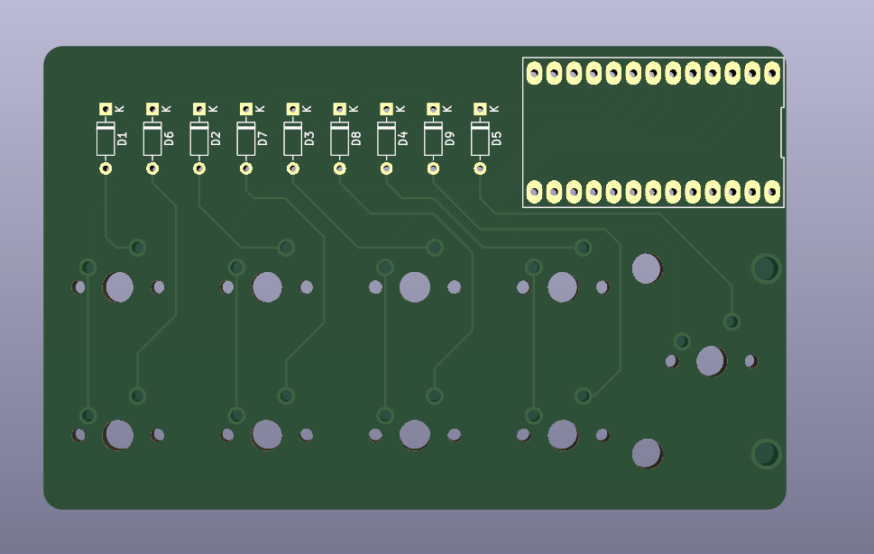
Nice! Now we have our board in a good place. One last step. Let's add "ground fills" connected to the ground net. I personally prefer the look of boards with ground fills. Practically, ground fills are important for signal integrity for all electronics. Since this is a carrier board, signal integrity isn't necessarily a big concern. The frequency of matrix scanning is only ~1KHz.
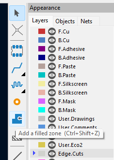
Click "Add a filled zone" and draw it a bit larger than the edge cuts of the board. Don't worry, there are default rules that will prevent the copper from actually being exposed on the edges.
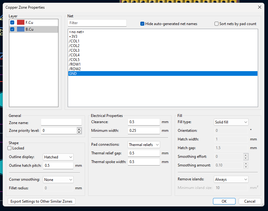
Select the top and bottom copper layers and select the "GND" net to connect the pours to ground. Be sure to change the clearance to 0.127mm
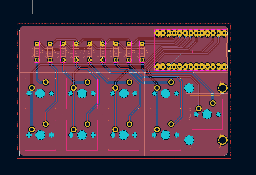
This should be the result! Let's take a look in the 3D viewer.
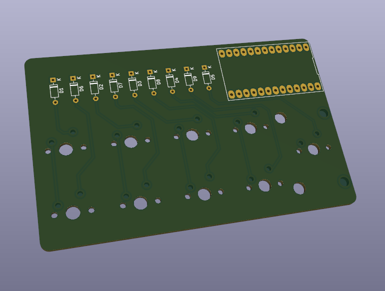
Congrats! Let's use Bouni's JLCPCB tool to generate board files.
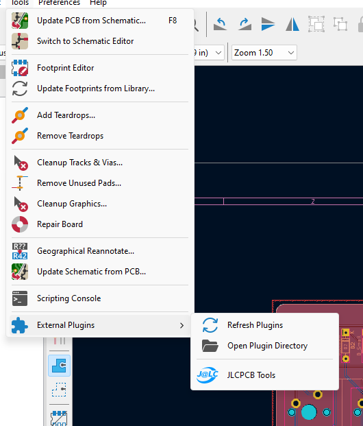
From the PCB editor, click "Tools > External Plugins > JLCPCB Tools."
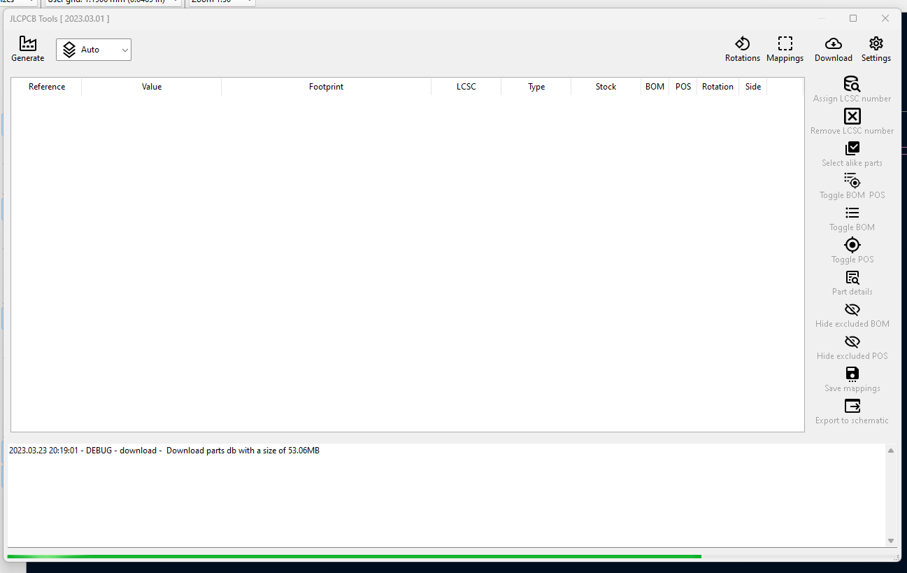
Allow it a moment to download the latest JLCPCB parts inventory. Then simply click "Generate" in the top left! We will explore more of the features of the JLCPCB Tools plugin in future posts.
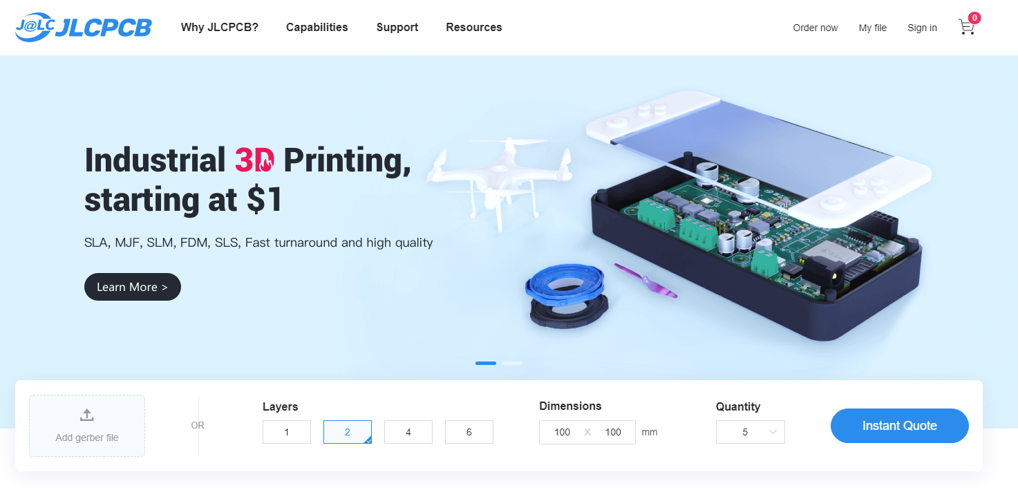
Navigate to https://jlcpcb.com and click "Instant Quote."
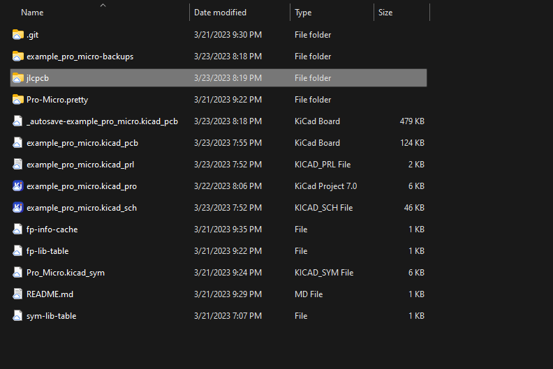
Next, open your project folder. You should see a new "jlcpcb" folder that contains your production files.

Open the "production_files" folder and then drag your "GERBER-*.zip" folder to the JLCPCB site.
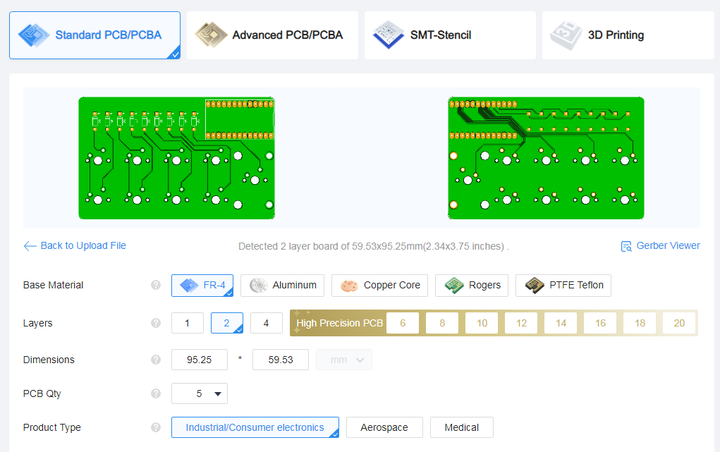
Let's use the defaults at first. We will explore other options in future posts.
The total cost for 5 boards comes out to ~$30. They should take about a week to arrive. I would recommend using DHL shipping.
In the next post we will design a plate + case for this macropad using KiCAD!
For more information and to ask keyboard specific or general electronics questions join our Discord!


