Keyboard Design Part 3 - Schematic Capture
It's time to get into the best part of keyboard design--coming up with a cool idea and bringing it to life. By the end of this post, we should be ready to start our PCB layout for a pro micro based keyboard.
To get started, lets play around with https://keyboard-layout-editor.com
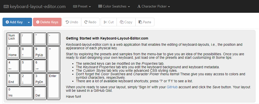
You will be greeted with the following interface.
Click on "Preset" in the toolbar and select "Blank Layout"
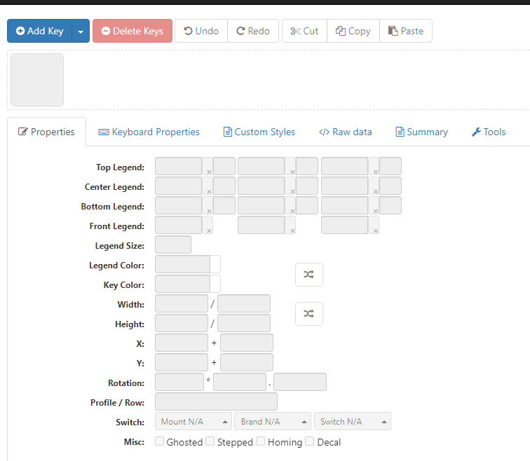
Let's add a few keys. Click the "Add Key" button to add a few keys. Play around!
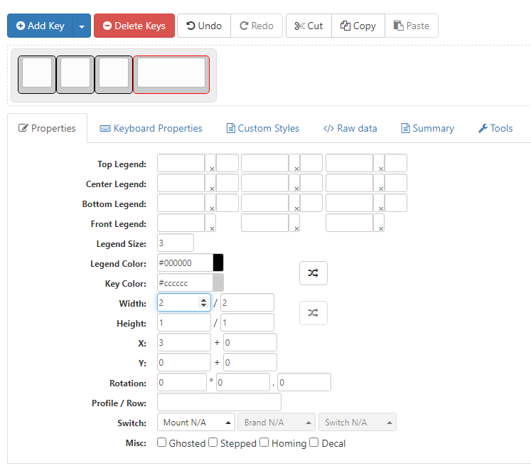
If you want to change the width of keys, click on it and modify the "width," and "height," properties.
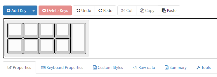
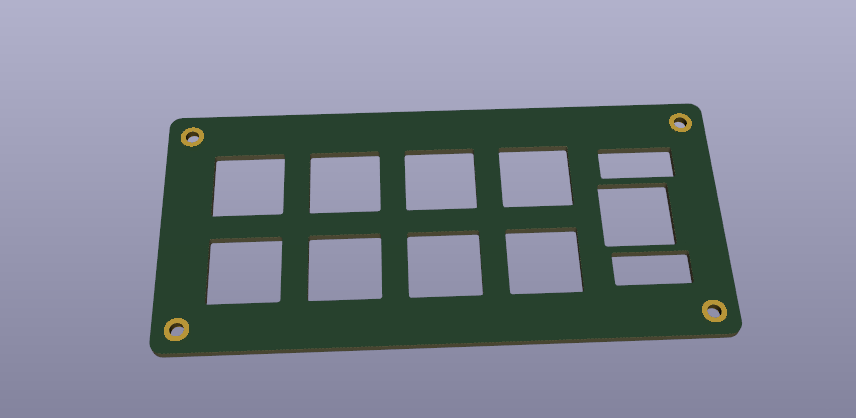
Here is my macropad design. Find something that you think looks cool!
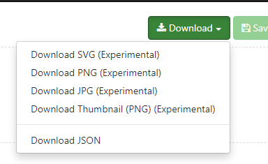
When you're ready, click "Download," in the top right and save the .json output to your project folder. This output can be used to create renders and will be helpful when creating our keyboard's QMK/Vial firmware.
Open up your KiCAD schematic.
Tip: to quickly open the schematic symbol placing dialog, use the shortcut "Shift+A"
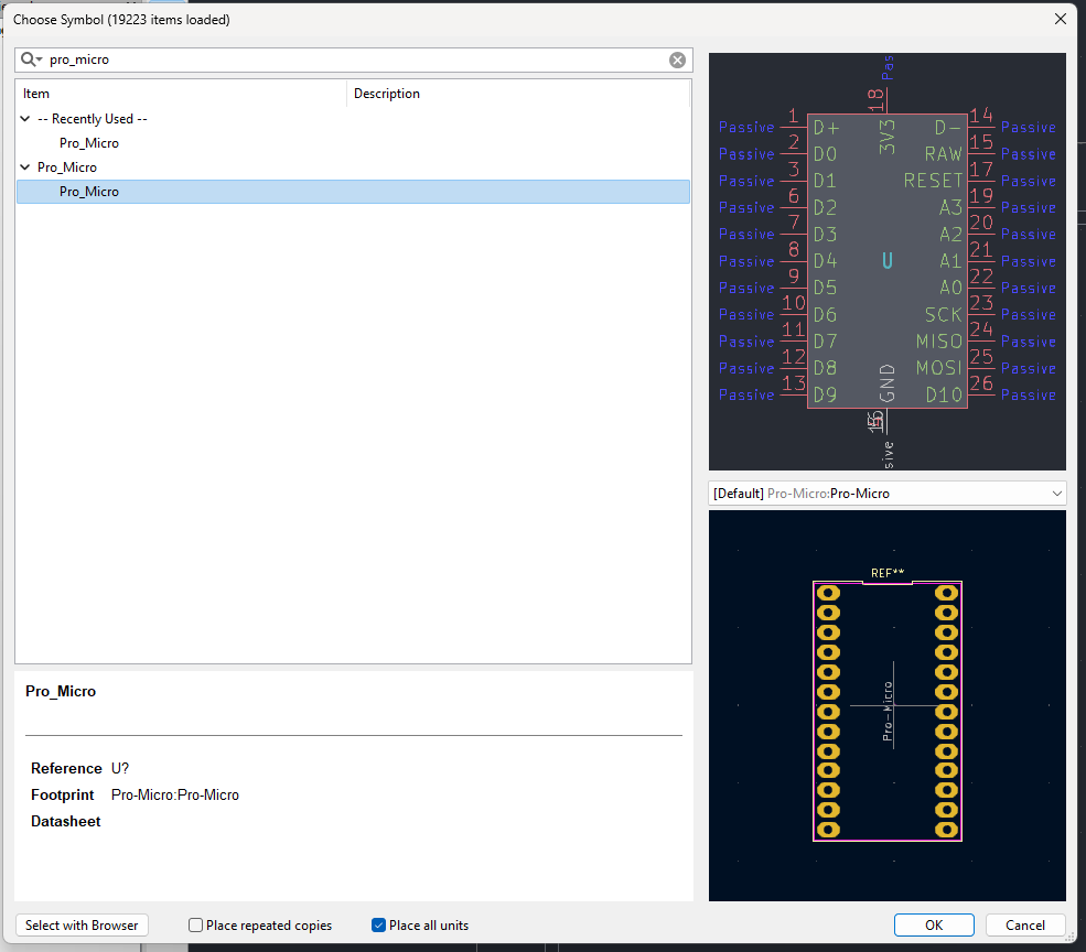
Search for the pro micro symbol you created in the last tutorial. If you don't have this, refer to Keyboard Design Part 2!
Press "OK," to place it on the schematic.
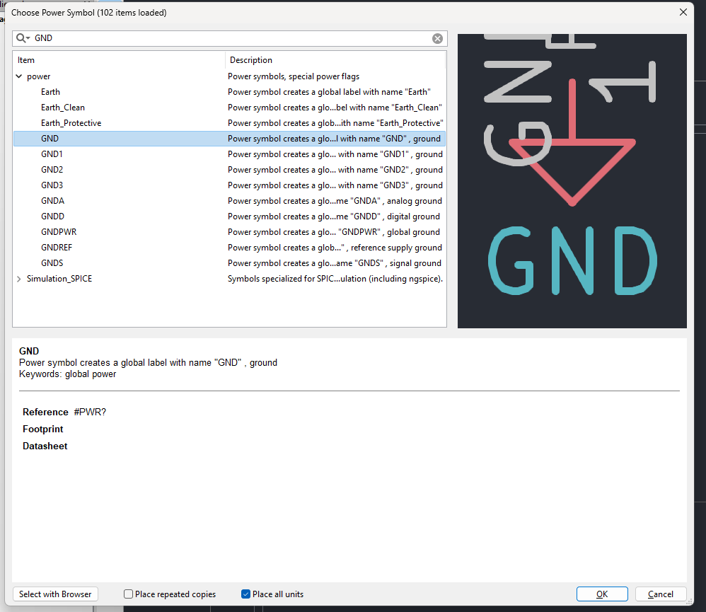
Next, press "P" to place power symbols on the schematic.
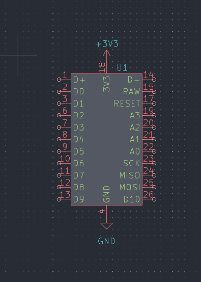
Search for GND and for +3V3 power symbols and place them on the top and bottom of the symbol.
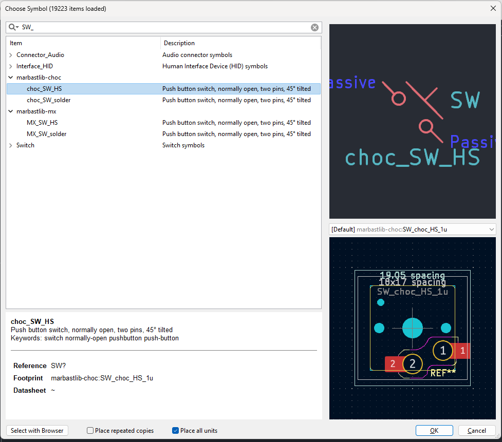
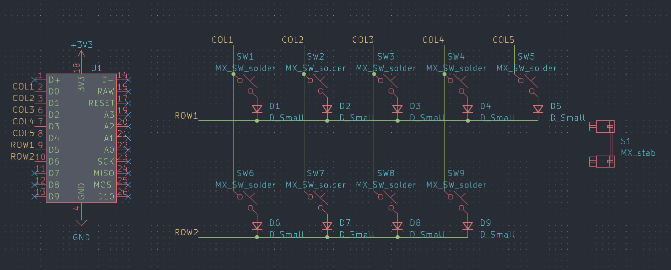
Now press "Shift+A" to add switches to the schematic. You can select either "solder," or "hotswap," switch symbols. These are just convenient ways that marbastlib has set up links between your footprint and symbol--in many other cases you will have to set footprint/symbol relationships as described in the previous tutorial. Also note the two different varieties of switch. "MX" switches are most commonly used but "choc" switches from Kailh have become increasingly popular for low profile keyboard designs. Both have hotswap footprint variants available.
If you are a beginner to soldering, I would recommend using the "solder" variant as it is easier (in the opinion of the author) to solder these switches as opposed to manually soldering hotswap sockets. In the future we will discuss how to order assembled keyboards with hotswap sockets.
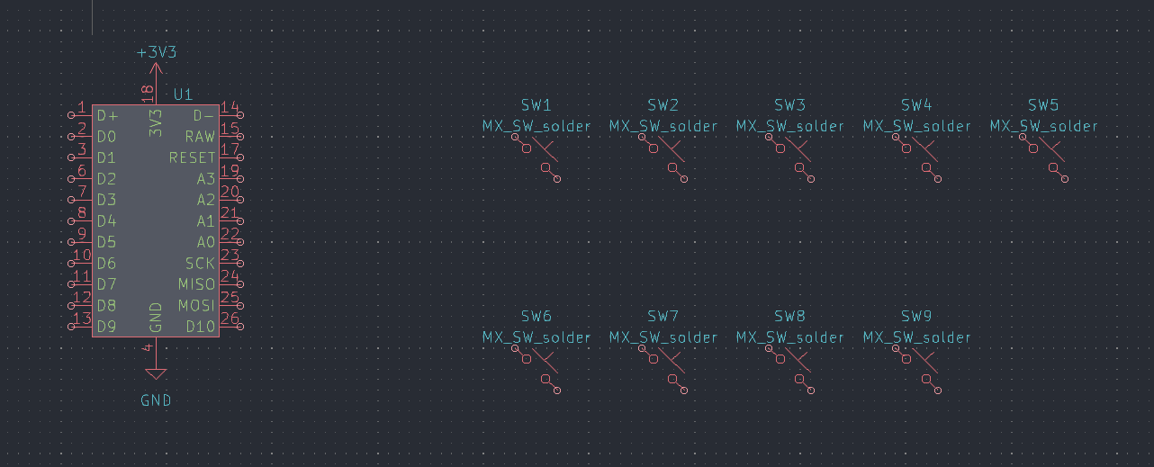
Add enough symbols to fill the keymap you created before. I typically place one symbol and then copy and paste as many as required.
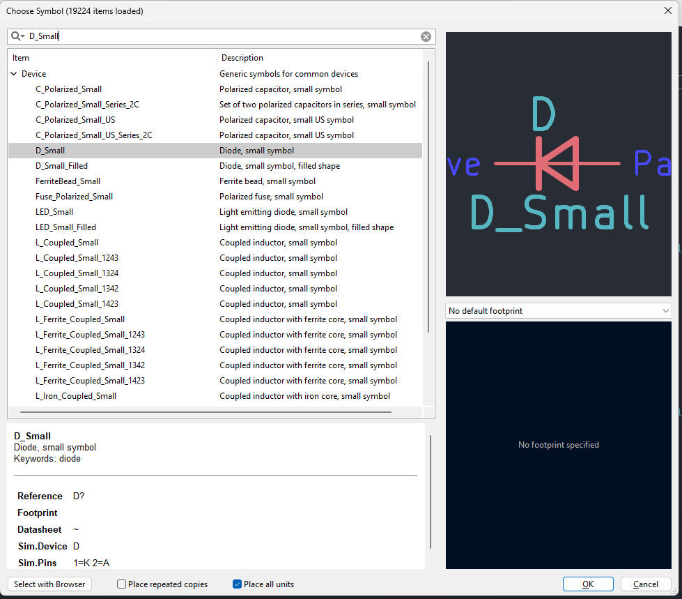
Next, add diode symbols to the schematic. Diodes are used so that modern matrix scanning algorithms will work properly. For more information, refer to the following page: https://pcbheaven.com/wikipages/How_Key_Matrices_Works/
In short, the diodes are added to prevent ghosting and to allow n-key rollover.
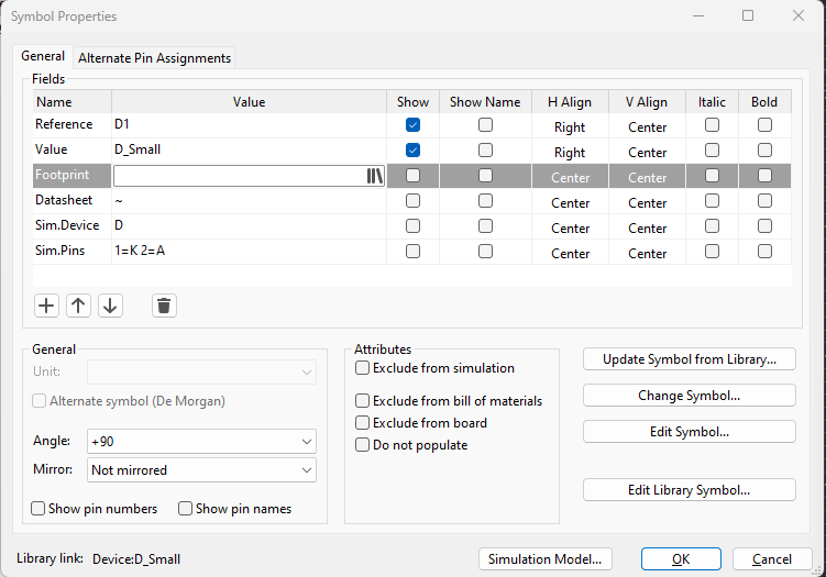
After adding the symbol to the schematic, double click on it and assign a footprint. The diode footprint depends on the specific diode you choose to use--in this case, we are using through hole diodes available on Adafruit.

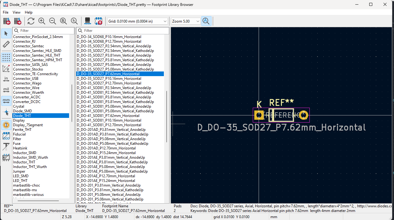
These are packaged in a "DO-35," formfactor. Refer to the datasheet to find this information for the diodes you choose to use.
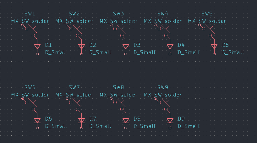
Continue populating your matrix.
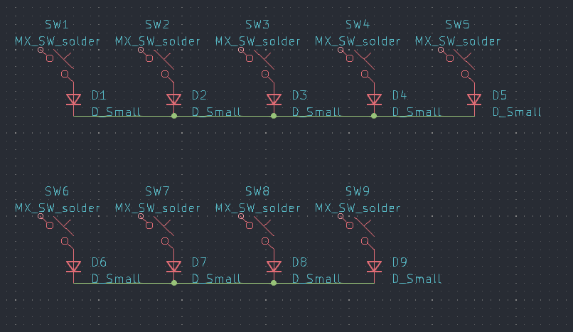
Once you have completed it, connect the "rows" of your keyboard to the cathodes of the diodes.
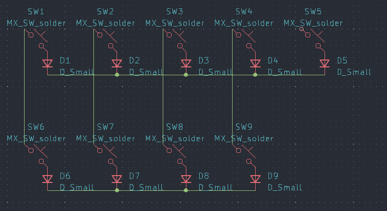
Connect the columns to the other side of the switches.
Click the "Add a net label" button (or press "L") and label the connections between rows and columns.
Once you have placed the rows/column labels, you can rotate them by pressing "R".
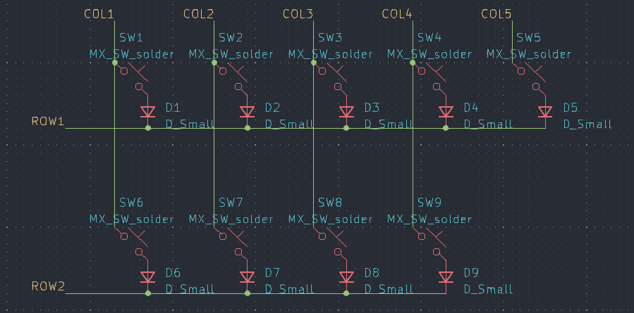
This completes the matrix layout.
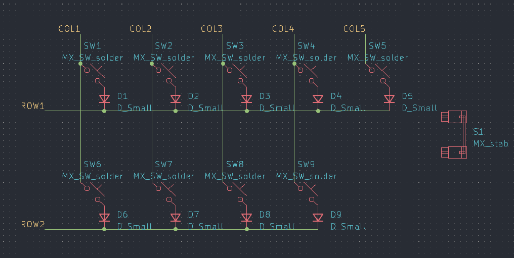
Good work! Just a few more details.
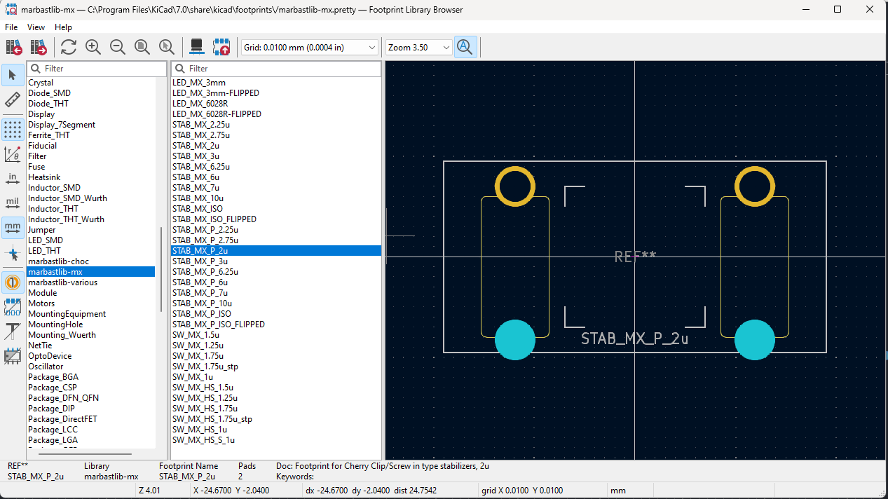
Add an MX_stab symbol from marbastlib. Double click on the symbol and change its footprint to the applicable stabilizer footprint.
Note: all keys >2 units in width/height require a stabilizer.
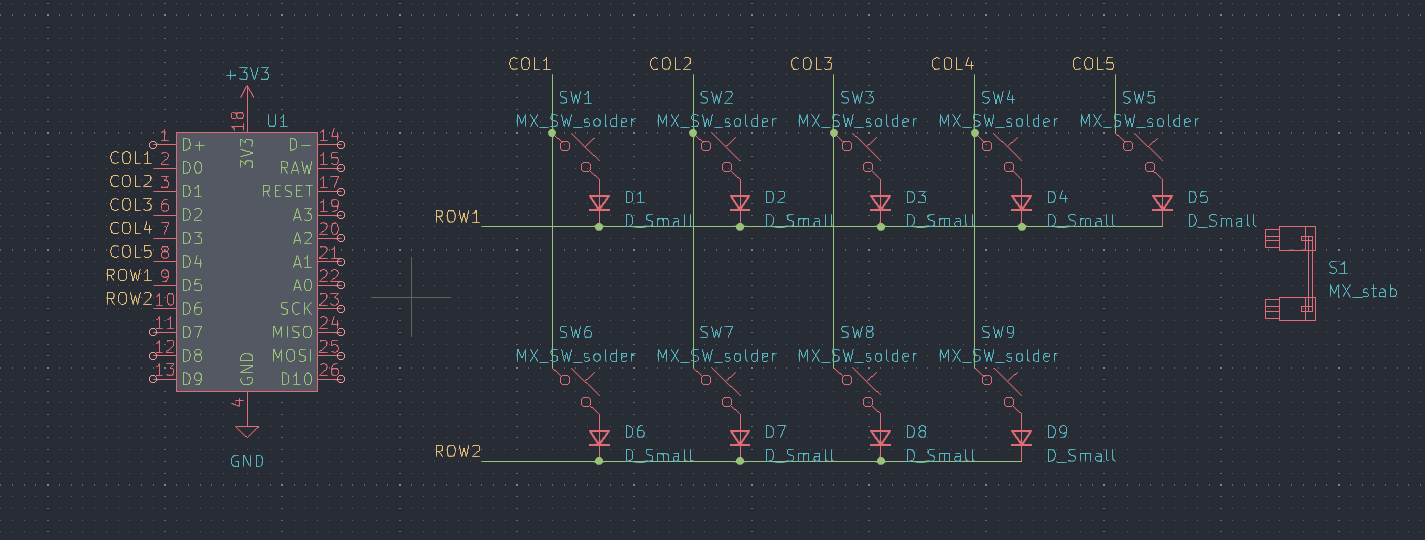
Copy your column and row labels to pins on the pro micro symbol. Be sure to select pins that are eligible GPIO pins as shown in the pinout image below.
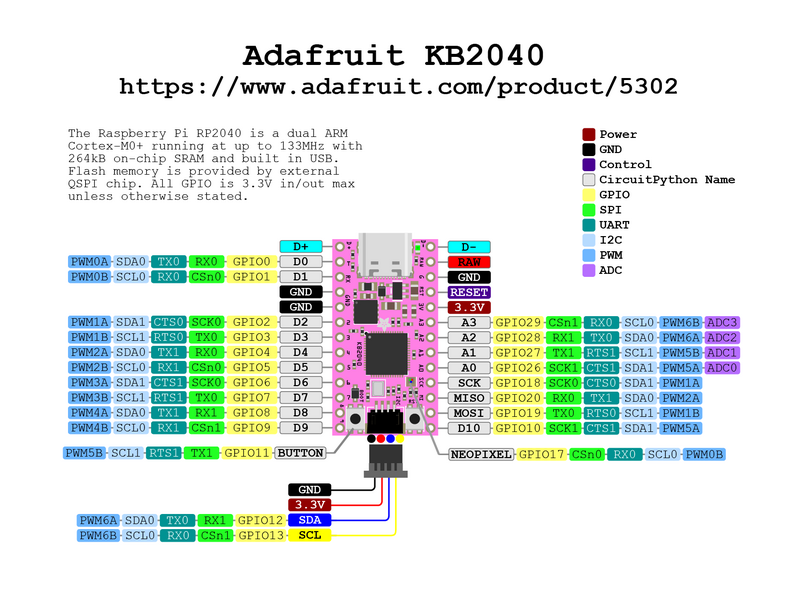
D2-D9 are pins we can use! To keep compatibility with other pro micro form factor devkits I would recommend using pins labeled "D*."
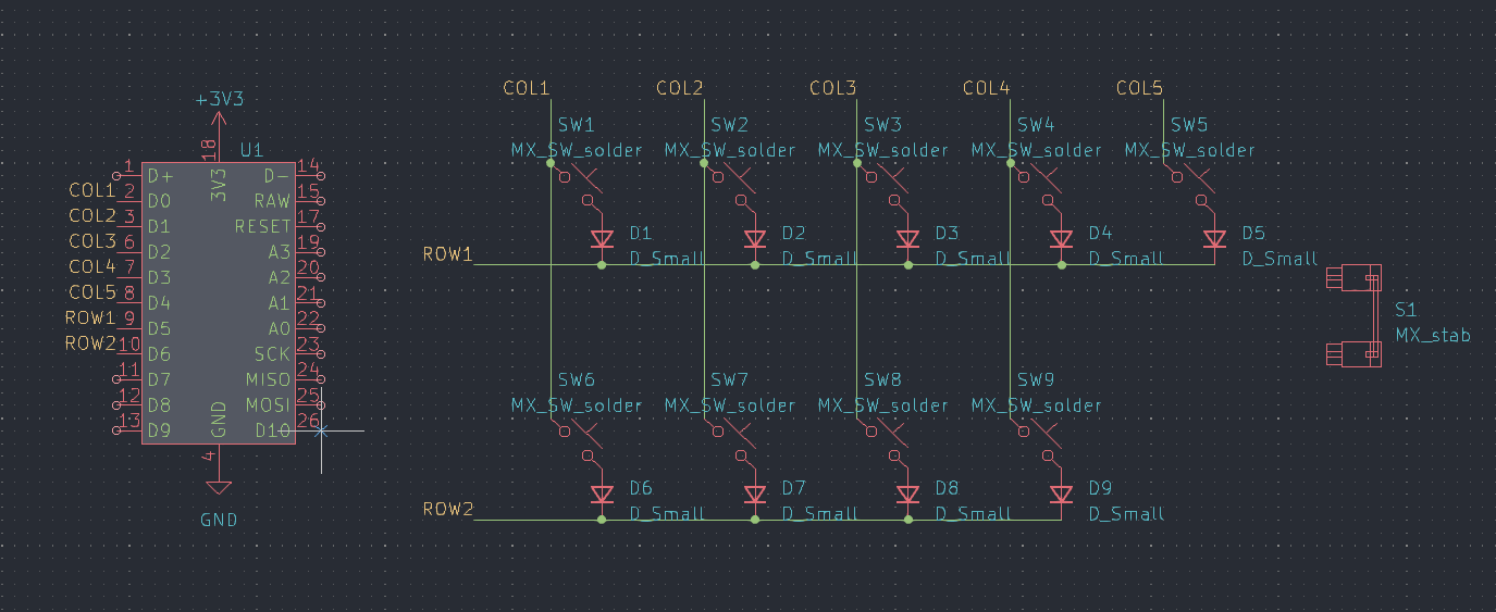
One last step--press "Q" over all unconnected pins to prevent an error in the design rules checker or "DRC." This adds a small "X" icon over pins that are not going to be routed in your PCB design.
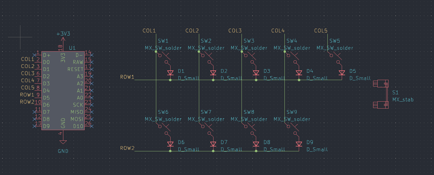
Congrats! You are one step closer to your first custom board design. In the next tutorial, we will learn a bit about the process of routing and ordering a PCB from JLCPCB!
For more information and to ask keyboard specific or general electronics questions join our Discord!

