Speedrunning Keyboard PCB Design or: How I Learned to Stop Worrying and Love the STM
Electronics design is supposed to be hard, isn't it? No longer.
Let's create a 40% PCB as fast as we can with nothing more than KiCAD, Keyboard Layout Editor, and a few scripts.
Let's create a fun KLE...
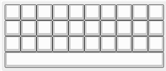
Download it to a safe place. You'll need it.
Start by cloning the following repo. I created it! If you run into issues, please open one!
Follow the instructions in the repo above to generate your schematic with all switches and diodes connected and labelled correctly. It may take a minute to run.
Copy the generated "generated_schematic.kicad_sch" to a fresh and clean new KiCAD project.
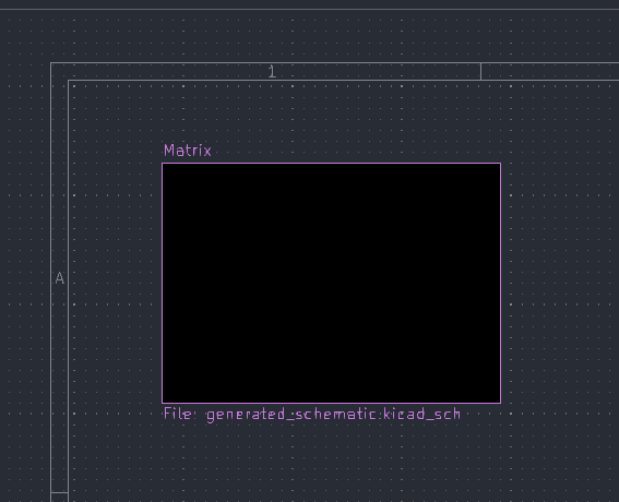
Add a hierarchical sheet:
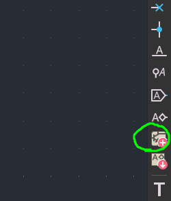
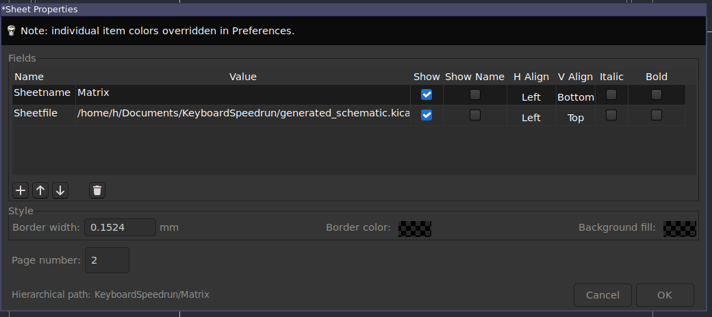
And select your sheetfile + name it something memorable.
Now let's quickly add a microcontroller, regulator, and USB-C port. Go go go!!!
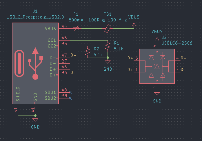
Add a USB-C port with the correct 5.1k pull down resistors. Include a series PTC fuse, ferrite bead, and ESD protection with the USBLC6-2SC6.
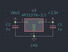
Add a regulator for the input USB power to step it down to 3.3V.
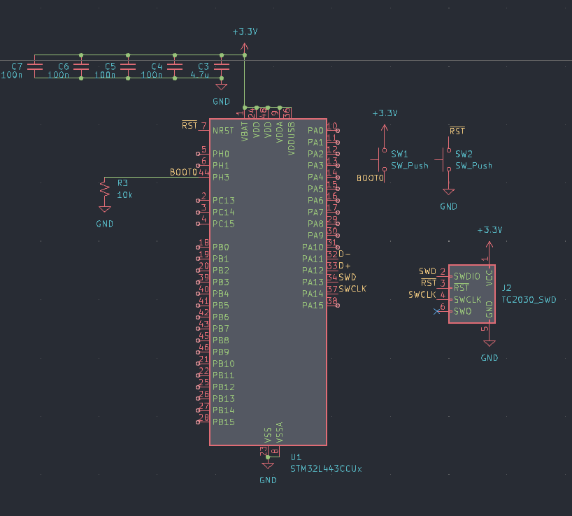
For this PCB, we're using the STM32L443CCU. This is a very easy chip to create a keyboard for as it requires few decoupling capacitors, has a USB bootloader, and requires no external crystal or termination resistors for USB.
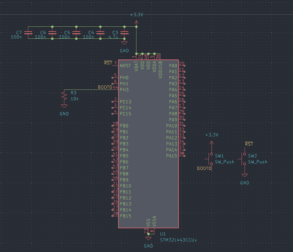
This is really it! All you need for an ARM microcontroller with 256k of flash, USB, and QMK/Vial support!
A few more niceties are in order. I'm adding a 6 pin tag connect port for SWD programming.
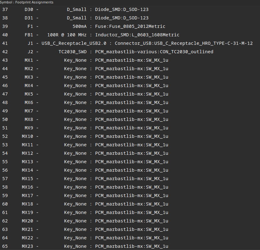
Now go through and assign your footprints. The switch footprints were automatically assigned but things like diodes, push button switches for reset, and capacitors will need to be set.
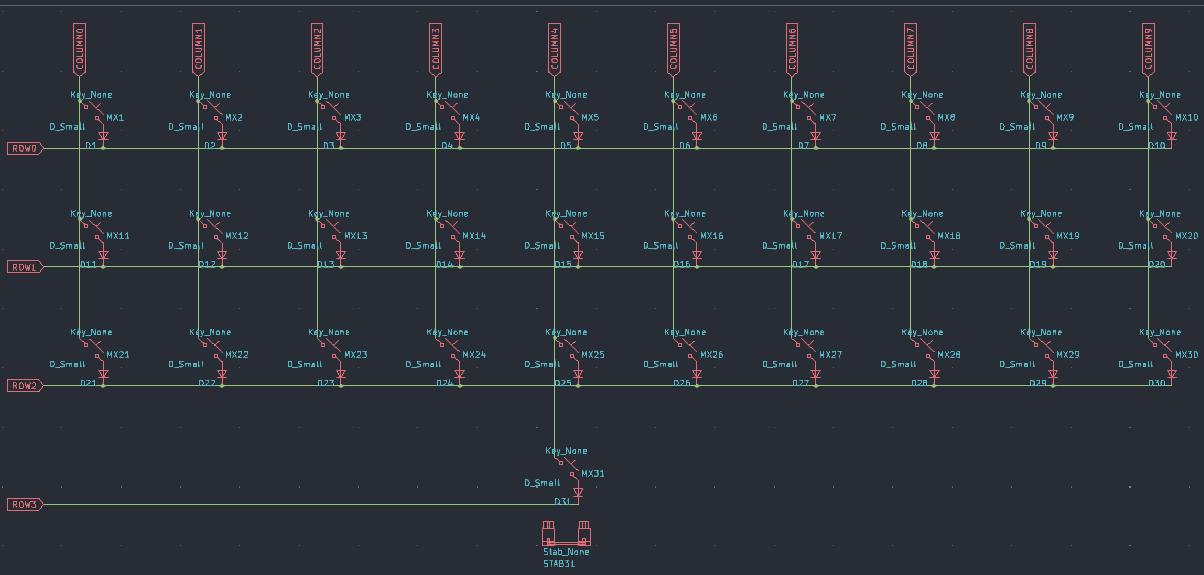
In your matrix schematic, connect the rows and columns and add global labels per row/column like so:
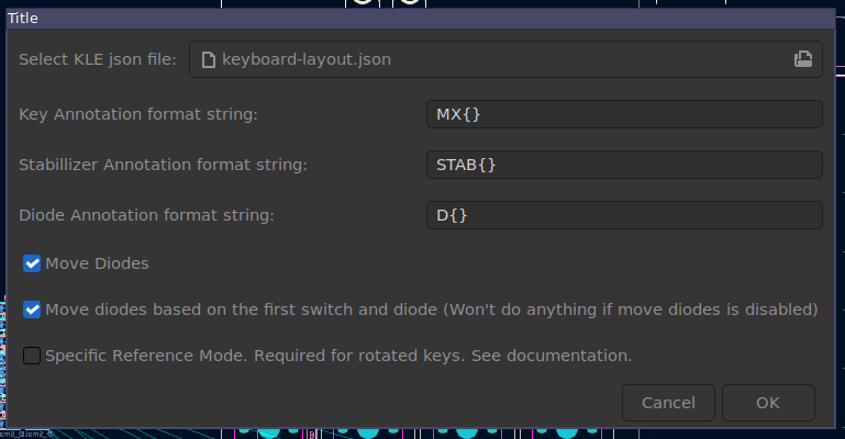
Next, install the following plugin from Zykrah:
Once you have it installed, add your keyboard-layout.json and change the key annotation and stab annotations to match my script (MX & STAB).

Your layout is ready! I'm going to flip the bottom stab and get to work routing my microcontroller:
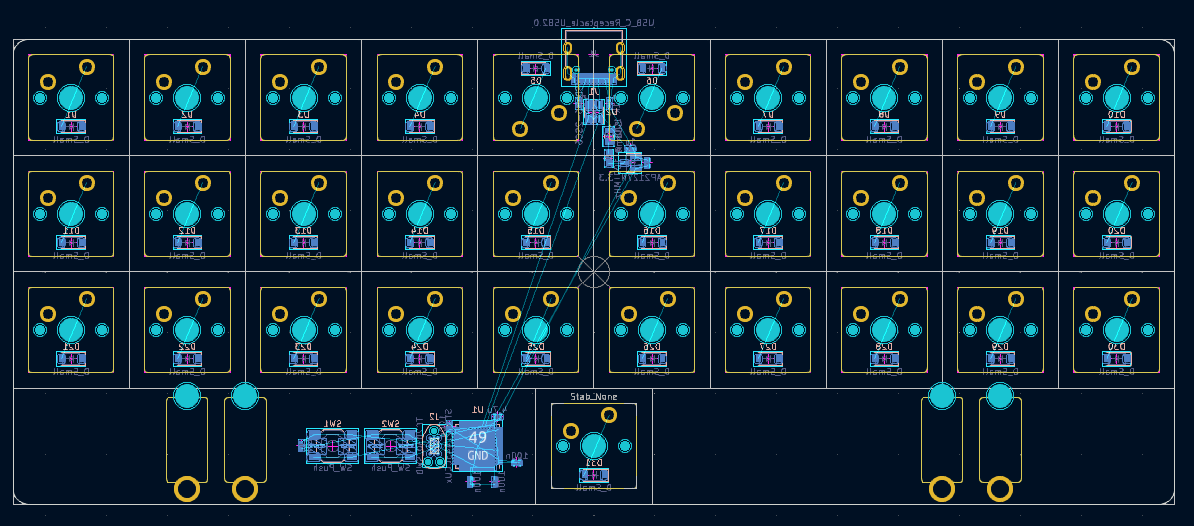
A few notes--I flipped the two switches up top to allow the USB port to sit correctly. I would recommend using a 4 layer board for all boards since they're so cheap from JLC. Keep traces out of your two inner layers and fill one with GND and one with VCC (3.3V in this case).
Here is the board, ready to be routed:
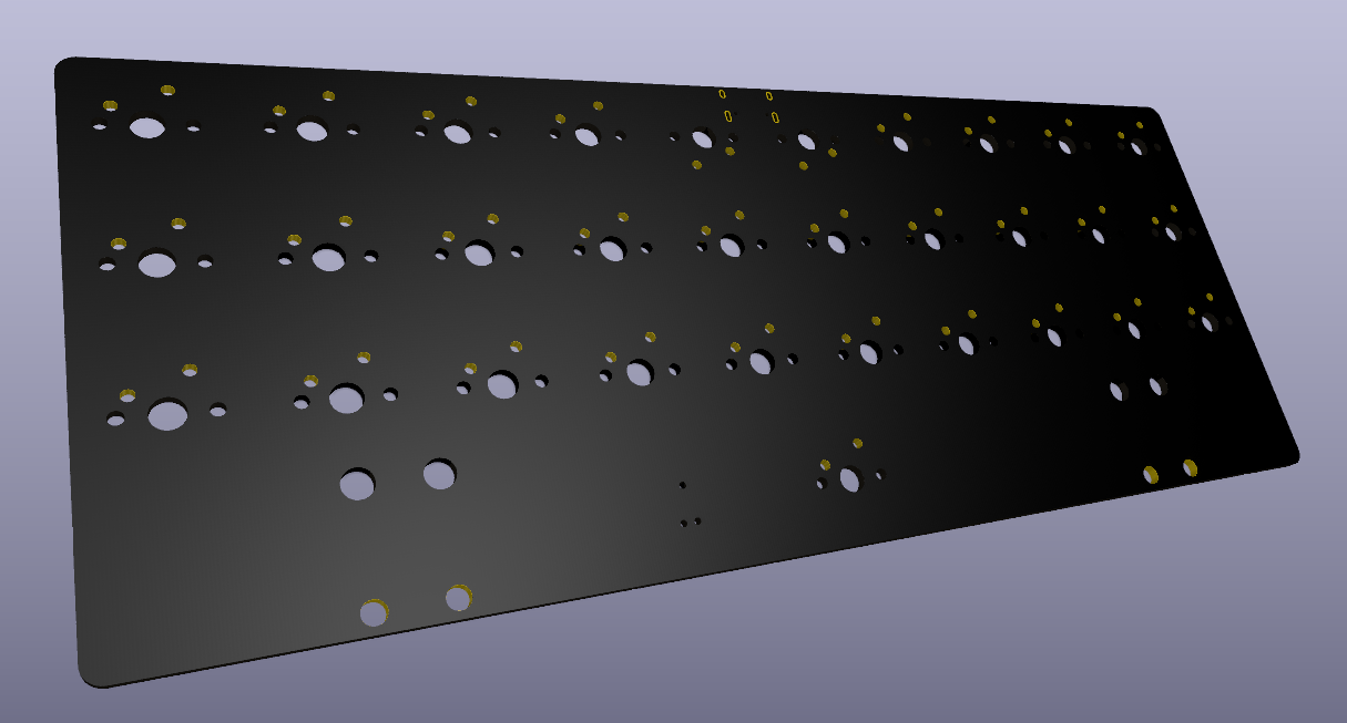
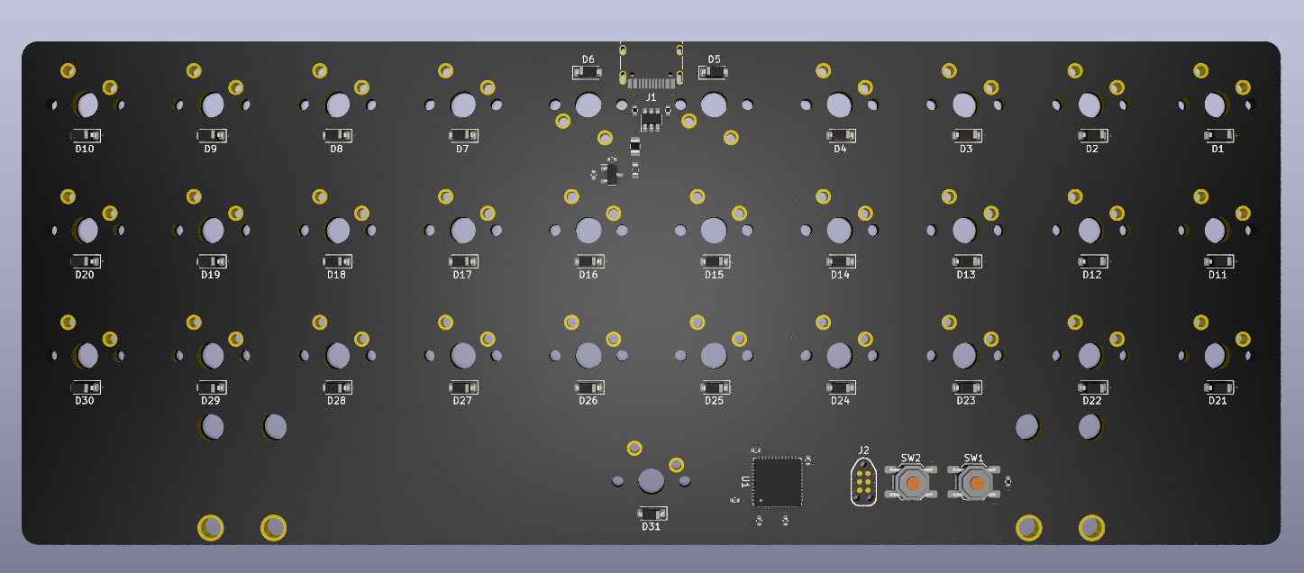
Once you have completed routing, generate your files with JLC. You may have to pre-order this ST part. Here's the complete board! Check the GitHub repo below for the full schematic, PCB, and production files.
Thanks for reading. Check out my Discord below!

